Photonic Integrated Circuit Design & Software

Where photonics moves from design to silicon.

Spark Photonics provides PIC design services and ready-to-run PIC Kits for defense, commercial, government, and academic institutions across the United States.

PICsFrom design to fab
4+Foundry platforms
USDefense & commercial
IPFull design ownership
Serving Defense & Government Commercial Technology Academic Research OEM & Startups Sensing & LiDAR

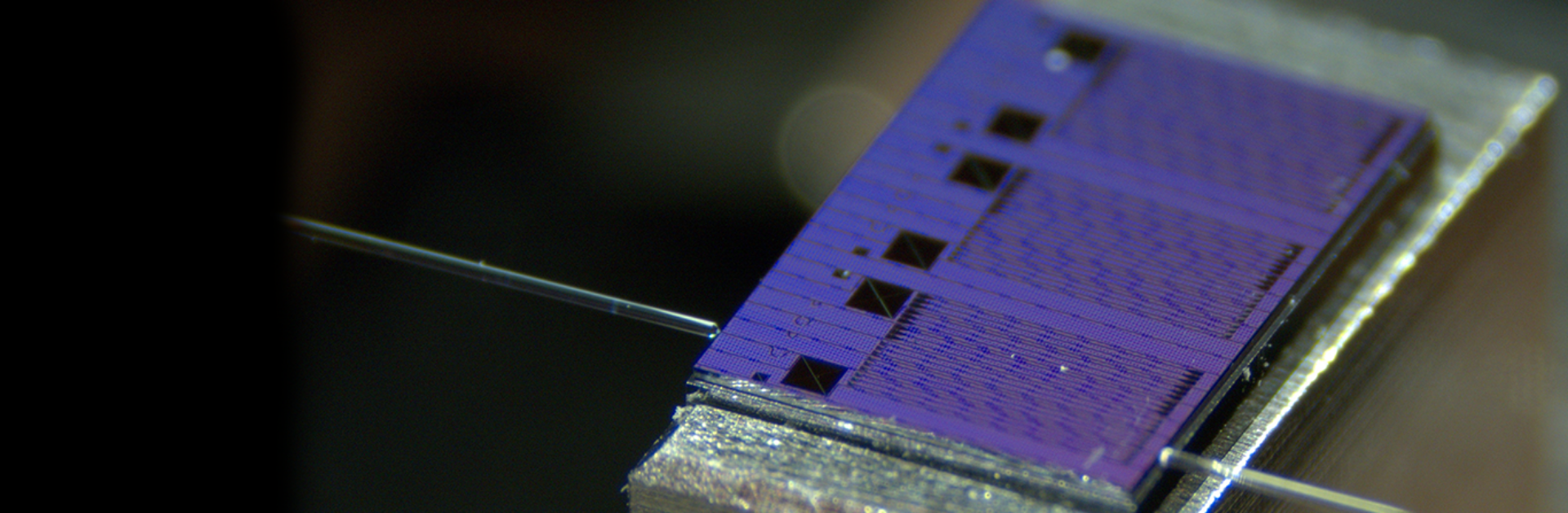
End-to-end PIC design, from concept to chip.

Two core offerings, scoped to where you are in development and what your foundry platform requires.

PIC Design Services

Full-stack photonic integrated circuit design tailored to your application. We cover architecture, component selection, layout, DRC, and fab handoff across silicon photonics, SiN, and InP platforms. Prototyping to production.

Start a project →

PIC Kits

Pre-validated, ready-to-order photonic component kits that accelerate your development timeline. Each kit ships with full documentation, layout files, and process design kit (PDK) compatibility notes for immediate integration.

Browse kits →

Design Consulting

Bring us in at any phase. Whether you need a design review, a second opinion on topology, or a partner to pick up a stalled effort, our team works alongside yours without displacing your IP or process knowledge.

Talk to an engineer →

Every kit validated on a real foundry PDK.

Spark PIC Kits give engineering teams a fast, reliable starting point. Pick the platform, order the kit, and get to characterization without rebuilding component libraries from scratch.

Request a kit datasheet
EWD Platform

EWD PIC Starter Kit

Edge Waveguide Design

The foundational kit for engineers working on the EWD platform. Includes optimized edge couplers, waveguide bends, splitters, and terminations, fully DRC-clean and ready for tape-out.

Edge Couplers 1x2 Splitter Bends Terminators
View kit details →
Modulator Suite

EWD Modulator Kit

High-Speed Electro-Optic

Electro-optic modulator building blocks for high-speed applications. Includes Mach-Zehnder structures, phase shifter segments, and RF electrode layouts with co-simulation support files.

MZM Topology Phase Shifters RF Electrodes Co-sim Files
View kit details →
Sensing & Detection

Photodetector Kit

Integrated Detector Structures

Germanium and silicon photodetector building blocks for on-chip detection. Covers butt-coupled and evanescent configurations with integrated bias pads and layout rules for heterogeneous integration.

Ge PD Si PD Butt-Coupled Evanescent
View kit details →
Routing & Coupling

MMI & Coupler Kit

Multi-Mode Interference

Optimized MMI splitters and directional couplers designed for flat spectral response and broad-band operation. Includes 1x2, 2x2, and asymmetric variants with tolerance analysis data.

1x2 MMI 2x2 MMI Dir. Coupler Tolerance Data
View kit details →
Grating Structures

Grating Coupler Kit

Fiber-to-Chip Interface

Focused grating coupler library for vertical fiber-to-chip coupling. Standard, apodized, and dual-polarization variants. Includes simulation results and coupling efficiency measurements from test chips.

Standard GC Apodized Dual-Pol Meas. Data
View kit details →
Full Integration

Complete PIC Dev Kit

End-to-End Development Bundle

Everything needed to build a functional PIC from scratch: edge couplers, passive routing, modulators, detectors, and MMIs in a single validated bundle. Ideal for first-time tape-outs or platform evaluation.

All Components Layout Bundle PDK Notes Support
View kit details →
"Integrated photonics moves fast. The teams that win are the ones who spend their time on application problems, not rebuilding foundry component libraries. That is what our kits are for."
Spark Photonics — Waltham, MA

From spec sheet to foundry submission in four steps.

A structured engagement keeps scope clear, iteration fast, and tape-out predictable.

01

Requirements

We gather your performance targets, foundry preference, timeline, and IP requirements. A kickoff call is usually enough to scope the work and identify any platform constraints up front.

02

Architecture & Simulation

Component selection, circuit topology, and full optical simulation before a single layout cell is drawn. We flag risk early and tune to your insertion loss and bandwidth targets.

03

Layout & DRC

Full GDS layout against the foundry PDK, DRC-clean and verified. We handle design rule constraints, fill strategies, and the documentation the fab needs for a clean submission.

04

Handoff & Support

You receive the complete design package: GDS, schematics, simulation data, and a handoff report. We stay available through the first fab run and assist with characterization interpretation.

Photonic integrated circuit chip detail

Designed for engineers who need answers, not a vendor pitch.

We are a small, technical team. There is no account management layer between you and the engineers doing the design work. When you ask a question, a photonics engineer responds.

  • Direct access to the engineers who designed your components
  • Platform-specific PDK knowledge across leading silicon photonics fabs
  • Realistic timelines and honest scoping, no padding for buffer
  • Full IP ownership transferred on project completion
  • Post-fab support through first characterization
Get in touch
Spark Photonics PIC chip
Spark Photonics Waltham, Massachusetts

A US-based PIC design firm built around application depth.

Spark Photonics is a photonic integrated circuit design services and software company. We work with defense agencies, commercial technology companies, government programs, and research institutions on the full range of silicon photonics design challenges.

The firm is based in Waltham, Massachusetts. Our work spans sensing, communications, LiDAR, quantum, and defense photonics. We are not a reseller or broker. Every design that leaves here was built by our team.

No managed services handoffs. You work directly with the engineers who understand your chip.
SiSilicon Photonics
SiNSilicon Nitride
InPIndium Phosphide
PDKMulti-Foundry

Tell us what you are trying to build.

Send the application, the platform, and a rough timeline. We will come back with a clear scoping proposal and any questions we need answered to get started.

Phone 617-519-6050
Email hello@sparkphotonics.com
Office 303 Wyman Street, Waltham, MA 02451

Start a conversation

HomePIC KitsEWD PIC Starter Kit
EWD Platform

EWD PIC Starter Kit

The foundational component library for edge waveguide design, validated on the EWD PDK and ready for tape-out without modification.

Kit Specifications

PlatformEdge Waveguide Design (EWD)
Waveguide CoreSilicon / SiN
Operating Wavelength1310 / 1550 nm
DRC StatusClean — verified
DeliverableGDS + documentation
SupportIncluded

Component library contents

  • Optimized edge couplers for lensed fiber and cleaved facet interfaces
  • Single-mode waveguide bends at multiple radii, loss-characterized
  • 1x2 and 2x2 Y-junction splitters with balanced output ports
  • Waveguide terminators for stray light suppression
  • Straight waveguide segments with fill-compliant layouts
  • Test structures for insertion loss and mode field measurements
Request full datasheet →

Platform and compatibility

The EWD Starter Kit was designed and verified against the EWD foundry PDK. All cells are DRC-clean and include the minimum required text labels, layer assignments, and keepout annotations for submission.

The kit ships as a GDS archive with a companion PDF design note covering insertion loss measurements from reference test chips, recommended integration rules, and known platform-specific gotchas.

Compatible with KLayout, Synopsys OptoDesigner, and Cadence Virtuoso via import. SPICE-compatible component models are provided where applicable.

Typical use cases

Sensing arraysLiDAR, spectroscopy
CommunicationsTransceivers, switches
DefenseRF photonics, EO
HomePIC KitsEWD Modulator Kit
Modulator Suite

EWD Modulator Kit

Electro-optic modulator building blocks for high-speed integrated photonics. Mach-Zehnder structures, phase shifters, and RF electrode layouts, co-simulation ready.

Kit Specifications

TopologyMach-Zehnder Modulator
ModulationElectro-optic (EO)
Data RateUp to 100+ Gbps
Electrode TypeCPW traveling-wave
Co-sim FilesIncluded (ADS / HFSS)
DRC StatusClean — verified

Modulator library contents

  • Single-drive and dual-drive Mach-Zehnder modulator topologies
  • Phase shifter segments in multiple lengths for VπL optimization
  • Coplanar waveguide (CPW) RF electrode layouts with ground shielding
  • Bias pad structures and DC contact configurations
  • Electro-optic co-simulation files for ADS and HFSS
  • S-parameter measurement reference data from test chips
Request full datasheet →

Where this kit is used

The EWD Modulator Kit is used in high-speed optical interconnects, microwave photonics, coherent transceivers, and electro-optic signal processing for defense systems. The CPW electrode layout is suitable for direct RF probe testing during wafer-level characterization.

Co-simulation files allow your RF team to work in parallel with photonic design, reducing back-and-forth iteration at the system integration stage.

HomePIC KitsPhotodetector Kit
Sensing & Detection

Photodetector Kit

Germanium and silicon on-chip photodetector building blocks. Butt-coupled and evanescent configurations with bias pad layouts for high-speed and high-sensitivity applications.

Kit Specifications

MaterialsGe, Si
ConfigurationButt-coupled + Evanescent
Wavelength Range1260 – 1625 nm
Bandwidth> 50 GHz (Ge)
Bias PadsIncluded
DRC StatusClean — verified

Detector library contents

  • Germanium p-i-n photodetectors, butt-coupled configuration
  • Silicon photodetectors for visible and near-IR detection
  • Evanescent-coupled Ge PD with tapered coupling region
  • Integrated bias pad layouts with RF-compatible ground planes
  • Dark current and responsivity measurement data from reference die
  • Heterogeneous integration layout rules and keepout annotations
Request full datasheet →

Where this kit is used

The Photodetector Kit is used in coherent receiver front ends, LiDAR receiver arrays, spectroscopic sensing systems, and optical power monitoring circuits. The evanescent configuration minimizes reflections at the detector interface, making it preferred for low-noise applications.

Each cell ships with process-verified dark current and responsivity data from test chips on the target platform, so you can close your link budget before submitting to fab.

HomePIC KitsMMI & Coupler Kit
Routing & Coupling

MMI & Coupler Kit

Optimized multi-mode interference splitters and directional couplers for broad-band, low-loss power splitting across your PIC design.

Kit Specifications

Topologies1x2, 2x2, Asymmetric MMI
Excess Loss< 0.3 dB typical
BandwidthC+L band
Imbalance< 0.2 dB
Tolerance DataIncluded
DRC StatusClean — verified

Splitter and coupler library

  • 1x2 MMI splitter, symmetric 50/50, optimized for minimal excess loss
  • 2x2 MMI coupler for balanced and cross-port configurations
  • Asymmetric MMI variants for uneven splitting ratios (30/70, 10/90)
  • Directional couplers with gap sweep design files for ratio tuning
  • Full tolerance analysis: width and etch depth variation studies
  • S-parameter simulation data and measured reference results
Request full datasheet →

Where this kit is used

MMI splitters are the backbone of most PIC topologies. This kit is used in optical phased arrays, coherent receivers, Mach-Zehnder interferometers, wavelength multiplexers, and power monitoring taps. The directional couplers complement the MMI library where wavelength selectivity is needed.

Tolerance analysis data lets your team assess yield risk against your foundry's typical process variation before tape-out, reducing costly respins.

HomePIC KitsGrating Coupler Kit
Grating Structures

Grating Coupler Kit

Fiber-to-chip coupling library for vertical and near-vertical incidence. Standard, apodized, and dual-polarization grating couplers with measured efficiency data from production test chips.

Kit Specifications

VariantsStandard, Apodized, Dual-Pol
Peak Efficiency> −1.5 dB (apodized)
3dB Bandwidth> 40 nm
Fiber Angle8° / 10° variants
Meas. DataIncluded
DRC StatusClean — verified

Grating coupler library

  • Standard uniform-period grating coupler, optimized fill factor
  • Apodized grating coupler for reduced sidelobe and improved efficiency
  • Dual-polarization grating coupler for TE/TM simultaneous coupling
  • 8-degree and 10-degree fiber angle variants for common test setups
  • Coupling efficiency vs. wavelength measurement data from reference die
  • Alignment tolerance analysis for automated fiber attachment
Request full datasheet →

Where this kit is used

Grating couplers are the primary test access point for nearly every PIC prototype. This kit is used in wafer-level test configurations, packaged module fiber interfaces, and systems where edge coupling is not accessible due to chip geometry.

The dual-polarization variant is specifically suited to coherent systems and quantum optics experiments where polarization state matters. The measured efficiency data lets you close the fiber coupling loss budget on day one.

HomePIC KitsComplete PIC Dev Kit
Full Integration

Complete PIC Dev Kit

Every component library in one validated bundle. Edge couplers, passive routing, modulators, detectors, and MMIs, packaged for teams starting a fresh tape-out or evaluating a new foundry platform.

Bundle Includes

EWD Starter KitIncluded
Modulator KitIncluded
Photodetector KitIncluded
MMI & Coupler KitIncluded
Grating Coupler KitIncluded
Engineering SupportPriority

Everything in one package

  • All five individual Spark PIC Kit libraries in a single GDS archive
  • Unified PDK notes document covering cross-kit integration rules
  • Example full-chip floorplan demonstrating component placement and routing
  • Priority engineering support for tape-out questions and DRC resolution
  • Complete simulation dataset for link budget closure
  • License for internal use on up to three tape-out projects
Request pricing →

Teams moving fast on a first tape-out

The Complete PIC Dev Kit is designed for engineering teams who cannot afford to spend two months building a component library before they can start designing their actual circuit. It eliminates the foundry PDK bootstrapping problem and gets your team to layout on day one.

It is also the right choice for organizations evaluating a new foundry platform. Rather than building test structures from scratch to characterize the process, you start with validated data and focus your tape-out budget on your actual application.

Priority support is included, meaning your questions go directly to the Spark engineers who built the kit. Not a support ticket queue.